 WiPDA-Asia
 Sponsored by the IEEE Power Electronics Society
IEEE Workshop on Wide Bandgap Power Devices and Applications in Asia WiPDA-Asia 2027
Three days in Kyoto on wide bandgap devices, their packaging and their applications, with academia and industry in equal measure.
Key dates
- Abstract submissionNovember 15, 2026
- Review notificationJanuary 10, 2027
- Final submission and registrationFebruary 12, 2027
The workshop
One room for device physics and the converter it ends up in
The Workshop on Wide Bandgap Power Devices and Applications in Asia (WiPDA-Asia) is sponsored by the IEEE Power Electronics Society. Device scientists, circuit designers, and application engineers meet in one place to share technology updates, research findings, development experience, and application knowledge.
The 7th edition runs on August 22-25, 2027 in Kyoto, Japan, and is the first under a dedicated Steering Committee for Asia. It is structured around three topics — devices, packaging and applications — and aims at a balanced mix of academia and industry in both its speakers and its audience. The venue is TBD.
Short courses
Learn the ground
One tutorial on each of the three topics opens the workshop, included in the full registration.
Keynotes
Hear where it is going
Pioneers of the technology and the people building on it now, from universities and from industry.
Technical papers
Show your work
Oral and poster sessions across the three days, with the proceedings submitted to IEEE Xplore.
Scope
Topics
Papers are welcome on anything in this list, and on work that does not fit it yet.
- Device structures and fabrication techniques
- Device characterization and modelling
- Advanced packaging solutions
- Robustness and reliability studies
- Novel and advanced applications (transportation, data centres, SSTs)
- Ultra wide-band-gap materials
- Gate drivers and auxiliary circuits
- High-efficiency, high-power-density converters
- AI and machine learning for WBG devices, packaging and converters
Keynotes
Speakers
-
Special Address
Prof. Hiroyuki Matsunami
Kyoto University of Advanced Science, Japan
-

Devices
Graduate School of Engineering, Kyoto University, Japan
Physical Understanding and Performance Enhancement of SiC MOSFETs
-
Devices
Dr. Kazuhide Ino
ROHM Semiconductor Ltd., Japan
-
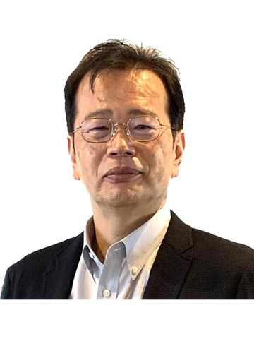
Packaging
Center for Innovative Integrated Electronic Systems (CIES), Tohoku University, Japan
Advanced Power Modules and Gate Control Technology for Maximizing the Performance of WBG Devices
-
Packaging
Dr. Shiori Idaka
Mitsubishi Electric Europe, Germany
-
Applications
Prof. Jin Wang
The Ohio State University, USA
-
Applications
Dr. Kimimori Hamada
Huawei Technologies Japan, Japan
Short courses
Tutorials
-

Devices
PowerAmerica / North Carolina State University, USA
Fundamentals of SiC Power Devices
-

Packaging
Division of Materials and Manufacturing Science, Graduate School of Engineering, The University of Osaka, Japan
Sintered joining for power devices − Microstructural analysis and local mechanical property evaluation
-

Applications
NexFi Technology Inc. / The University of Osaka, Japan
Pushing Solid-State Pulsed Power Beyond 10 kV: Series-Connected SiC MOSFETs and Advanced Applications